Technology
How Do FPGAs Work: A Clear Breakdown
15. 7. 2025

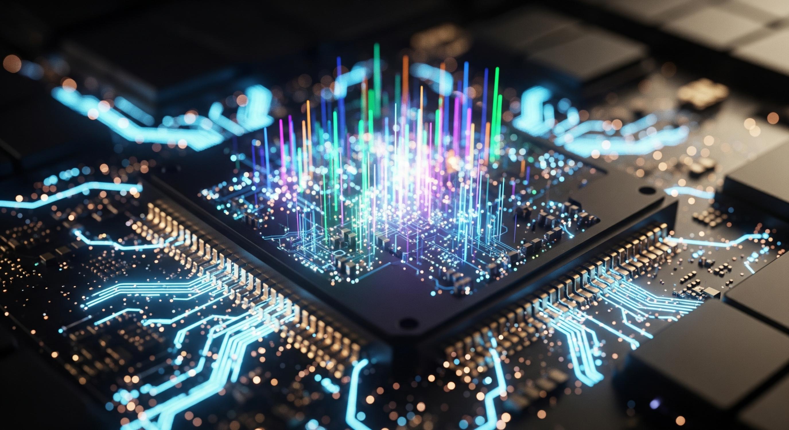
Pursuit of speed has propelled Field Programmable Gate Arrays (FPGAs) to the forefront of trading technology. Why are these chips so valued? It’s their ability to create customized hardware circuits that are adaptable, reprogrammable, and built to accelerate calculations exactly as needed.
The foundation of every FPGA lies in its configurable logic blocks (CLBs). You'll find up to millions of these units in one device. Though manufacturer terminology can vary. Intel calls them Logic Elements (LEs), Xilinx refers to them as CLBs, but the concept remains the same.
Each CLB houses essential elements: lookup tables for creating custom logic functions, flip-flops for storing digital states, multiplexers for creating wider functions, and specialized carry chains for arithmetic. What’s remarkable is the programmable nature of these blocks. With FPGA configuration, the same CLB might function as a simple logic gate in one setup or as part of a complex mathematical operation in another.
This adaptability is what sets FPGA architecture apart. Need a circuit tweaked for your specific application? With FPGAs, you can reorganize thousands of CLBs to meet those exact requirements.
To fully understand the power and flexibility of a CLB, it's helpful to look at its internal structure. Each CLB is composed of several basic digital elements:
- Look-Up Tables (LUTs): At the heart of logic implementation, LUTs act as small on-chip RAMs storing a truth table for any combinational logic of their input size. Most modern FPGAs use 4-input, 5-input, or 6-input LUTs, with 6-input LUTs becoming more standard. A 6-input LUT can handle any logic function of six variables, covering most common digital needs. For more complex logic, multiple LUTs are interconnected through the FPGA’s programmable interconnect network.
- Flip-Flops (Registers): These are one-bit memory cells used for storing state information and implementing sequential logic—essential for circuits like shift registers, counters, and finite state machines. Flip-flops are driven by clock signals, providing synchronization and enabling stateful behavior.
- Multiplexers: Dedicated elements for combining the outputs of LUTs to create even wider logic functions while achieving efficient resource utilization.
- Carry Logic: To speed up arithmetic operations, modern CLBs include specialized carry logic chains. These dedicated pathways accelerate addition, subtraction, or comparison operations, reducing delay and resource usage compared to building arithmetic only from basic LUTs.
These core components work in tandem to allow each logic block to serve many possible roles within a circuit, from simple gates to parts of complex arithmetic or control units. The particular structure, how many LUTs, flip-flops, multiplexers, and what kind of carry logic, varies by FPGA family and vendor. Advanced FPGAs may include "fracturable" LUTs, which can be split into smaller, independently configurable logic units for greater packing efficiency and performance.
This internal flexibility also impacts the density and breadth of functionality an FPGA can achieve. The size, number, and arrangement of these elements directly affect how much logic, memory, or computation can be implemented, and how fast and efficiently it operates.
When you look at the overall FPGA architecture, think of it as a highly organized network of programmable components. The CLBs are packed and connected by a web of interconnects, while input/output (I/O) blocks anchor the edges, interfacing the FPGA with the outside world.
The programmable interconnect network is a crucial enabler of FPGA flexibility. It comprises various routing resources, optimized for different signal distances and speeds. Short wires connect nearby CLBs for minimal delay, while longer routes traverse the chip for more distant communication. Global routing networks also ensure that critical signals, such as clocks, reach every part of the device precisely.
Programming these interconnects is what turns a generic, reprogrammable FPGA into a specific, functioning digital circuit. Routing tools activate programmable switches to create the exact signal paths needed for your design. This routing can be complex, especially as designs grow larger and more sophisticated.
Surrounding the core logic, I/O blocks act as gateways. These modules support a wide range of standards and voltages, making it possible to directly connect FPGAs with memory, processors, network modules, sensors, or other digital devices. Modern I/O blocks may also offer advanced features like adjustable drive strength, on-chip termination, and high-speed serializers necessary for multi-gigabit communication.
While logic blocks and LUTs offer flexibility, certain advanced functions need more than just programmable logic. Modern FPGA architecture addresses this with specialized resources.
Block RAM (BRAM) is distributed throughout the FPGA, providing dual-port, on-chip memory for storing or buffering data. Why is this important? Having fast local memory dramatically accelerates tasks like signal processing and data buffering, cutting reliance on slower external memory resources.
Digital Signal Processing (DSP) slices are another key addition. These hardened multipliers, adders, and accumulators are optimized for mathematical operations, essential for applications ranging from machine learning to communications. Using DSPs frees up general logic blocks and helps push performance even higher.
High-speed serial transceivers have also become commonplace, letting FPGAs communicate with other components using industry standards like PCI Express, Ethernet, or SATA. These transceivers handle the tough analog requirements of high-speed signaling, allowing FPGAs to directly communicate at multi-gigabit rates with minimal extra hardware.
With these resources, FPGAs have evolved from simple programmable logic devices to complete computing platforms. Today, many FPGAs resemble system-on-chip (SoC) solutions, combining the flexibility of programmable logic with the speed and efficiency of hardened blocks.
What does the workflow look like for programming FPGAs? It starts with a design entry, most commonly using a hardware description language (HDL) such as Verilog or VHDL. Here, engineers describe their circuits' structure and logic. Alternatively, high-level synthesis tools can translate C or C++ into HDL, opening FPGA development to those more familiar with software programming.
Next comes synthesis. The FPGA design tool translates HDL into a netlist of primitive logic elements, optimizing the design for the specific FPGA architecture. This stage targets not just functionality, but also resource usage, timing, power, and performance.
After synthesis, the placement and routing phase begins. This process assigns each logic element to a specific location on the chip and determines how they’re physically interconnected using the FPGA's programmable fabric. Achieving optimal performance while utilizing resources efficiently makes this step particularly demanding.
The final step is bitstream generation: creating a binary file that encodes every configuration choice for the FPGA, down to each configurable logic block and routing path. Loading this bitstream programs the FPGA hardware into the exact circuit that was designed.
⏩ Watch how our FPGA solution accelerates high-frequency trading.
With so many digital technology options, when does an FPGA make sense? If you need flexibility and high-speed parallel processing, FPGAs are often the best choice.
The key advantage is in-field programmability. FPGAs can be reconfigured after deployment, adapting to new standards, algorithms, or even bug fixes. For industries like telecom or AI, this means longer product cycles and easier adaptation to evolving technologies.
Parallelism is another major strength. Unlike CPUs, which are fundamentally sequential, FPGAs can process hundreds or thousands of operations at the same time.
FPGAs also dramatically cut time-to-market compared to developing a custom application-specific integrated circuit (ASIC). While ASIC projects can take years from concept to production, FPGAs allow you to develop, test, and deploy in weeks or months.
In high-performance, cutting-edge sectors such as financial trading, FPGAs offer a uniquely powerful solution by combining reprogrammable hardware and massive parallelism. Magmio simplifies their deployment by bridging ultra-low-latency hardware with flexible software integration, making it faster and more efficient to implement FPGA-based systems in demanding environments.
FPGAs are reprogrammable chips that create customized, adaptable hardware circuits to accelerate specific calculations. They utilize a massive network of configurable logic blocks that can be reorganized to meet exact application requirements. This in-field programmability allows systems to adapt to evolving technologies and updates after deployment.
FPGAs dramatically reduce time-to-market, allowing development and deployment in weeks rather than the years required for ASIC production. Their hardware is reprogrammable after deployment to adapt to new standards or bug fixes. FPGAs are also more cost-efficient for low-volume deployments.
The foundation of an FPGA consists of configurable logic blocks (CLBs), programmable interconnects, and input/output (I/O) blocks. CLBs contain essential elements like lookup tables, flip-flops, multiplexers, and carry chains for custom logic and arithmetic. A web of interconnects links these blocks, while I/O blocks interface the FPGA with external devices.
The workflow begins with describing circuit logic using a hardware description language (HDL) or high-level synthesis tools. Design tools then synthesize this code into a netlist, optimizing for resource usage and performance. Finally, a placement and routing phase assigns physical locations before generating a binary bitstream to configure the hardware.
LUTs act as small on-chip RAMs that store a truth table for combinational logic operations. Modern FPGAs typically use 4-input to 6-input LUTs, with 6-input variants handling any logic function of six variables. For highly complex logic, multiple LUTs are linked together through the FPGA’s programmable interconnect network.
Modern FPGAs integrate specialized resources like Block RAM (BRAM) for fast on-chip data storage, minimizing reliance on slower external memory. Digital Signal Processing (DSP) slices provide hardened components to accelerate mathematical operations. Furthermore, high-speed serial transceivers enable direct, multi-gigabit communication using industry standards like PCI Express or Ethernet.
Magmio simplifies FPGA deployment by enabling software developers without previous hardware experience to program FPGAs and achieve ultra-low latency for their trading strategies. The framework includes highly optimized IP cores for processing exchange protocols, which are linked with the customer strategy implemented in C++ using High-Level Synthesis (HLS) or HDL. On the host side, Magmio C++ API abstracts the user from low-level hardware details and provides easy communication between the FPGA card and customer software.


